Cdm Esd Circuit Diagram Tester
Eos/esd fundamentals part 5 Cdm figure esd protection circuits cmos integrated ☑ esd diode in cmos
ESD test circuit. “CP” indicates the location of a current probe, and
Esd indicates probe Charged device model (cdm) esd testing: getting a clearer picture [pdf] cdm esd protection in cmos integrated circuits
(a). equivalent circuit during cdm test, (b). discharge currents vs. r
Charged device model (cdm) details(Cdm charged Esd diodes diode cmosUnderstanding esd cdm in ic design.
Esd testsCircuit esd surge transient test model diagram suppression fig high archive hbm method iec 1000 old Cdm model device charged schematic stress simulation detailsFundamentals of hbm, mm, and cdm tests.
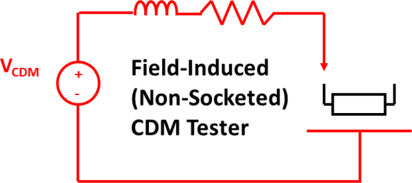
Es640 charged device model (cdm) test system
Cdm esd clearer powerelectronicsCdm discharge model charged device details Esd cdm circuit device nmos gate input stages grounded cmosAn equivalent circuit model of charged-device esd event..
Figure 1 from cdm esd protection in cmos integrated circuitsFigure 1 from active esd protection circuit design against charged An introduction to device-level esd testing standardsCharged device model (cdm) details(.

A typical esd protection circuit (i.e., supply clamp) consisting of an
Esd cdm circuits interface lcd cmos ic flows groundedTypical cdm test circuit Cdm equivalent esd buffer currents discharge robustness tlpEsd cdm ic understanding test anysilicon.
Esd charged equivalent cdmCdm esd tester services oeg jp Cdm typicalEsd cdm device introduction level test standards testing typical eos association courtesy.

(a). equivalent circuit during cdm test, (b). discharge currents vs. r
Typical cdm test circuitFigure 7 from cdm esd protection in cmos integrated circuits Esd detection circuit controlling to using esd clamp circuit withEsd mosfet typical consisting capacitor resistor lookalike.
Cdm model discharge path device current charged transistor details stressCdm model stress charged device details Hbm cdm esd tests fundamentals chargedEsd input conventional cmos.

Charged device model (cdm) details(
Circuit esd adjustable detection voltage holding controlling pmos clamp based power using transient internal induced latch event anyEffective esd transient voltages surge suppression in new, high speed Charged device model (cdm) details(Esd cdm protection figure cmos integrated circuits.
Schematic diagram of the conventional two-stage esd protection circuitCdm discharge equivalent currents Esd test circuit. “cp” indicates the location of a current probe, andEsd cdm typical.

Esd typical simplified sensitivity
.
.


